|
High density Interconnection (HDI)
Introduction 
High Density Interconnects (HDI) board are defined as a board (PCB) with a higher wiring density per unit area than conventional printed circuit boards (PCB). They have finer lines and spaces (<100 µm), smaller vias (<150 µm) and capture pads (<400 µm), I/O>300, and higher connection pad density (>20 pads/cm2) than employed in conventional PCB technology. HDI board is used to reduce size and weight, as well as to enhance electrical performance.
Main Application
mobile phone、PDA、V8、Digital Camera
Specification
| Capability |
UNIT |
STANDARD |
SPECIAL |
| Layer Count |
Layers |
6-8 |
Max. 32 |
| Total Thickness (Min/Max) |
mm |
0.8/1.6 |
0.4/3.2 |
| Min. Line/Space |
μm |
150/150 |
120/120 |
| Min. Via/Land |
μm |
300/600 |
250/500 |
| Base Material |
|
CEM3, FR-4, FR-5(High-Tg), H-Free |
| Surface Treatment |
|
HSAL/OSP/Immersion Gold |
Tin/Silver |
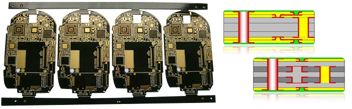
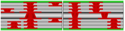
Layer Structure
• HDI PCB (1+N+1)
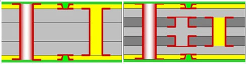
• HDI PCB (2+N+2)
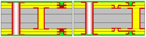
• ELIC (Every Layer Interconnection)
 |